Etching
Explore SPT’s high-performance dry etching technologies designed for MEMS, TSV, and compound semiconductor applications.
Etching Overview
Etching is a core process in semiconductor fabrication, enabling the precise removal of materials to define patterns and structures on a wafer.
SPT specializes in plasma-based dry etching (Si DRIE, RIE) and sacrificial layer etching engineered for high aspect ratio structures, low damage, and process uniformity in MEMS and advanced devices.
What is Etching in Semiconductor Manufacturing?
Etching is the process of removing specific material layers from a semiconductor wafer to form patterns defined by a mask.
There are two primary types: wet etching, which uses liquid chemicals, and dry etching, which uses plasma or reactive gases in a vacuum.
SPT focuses on dry etching technologies, offering precise and clean pattern transfer for complex structures such as MEMS, TSV, and compound semiconductors.
Types of Etching: Dry vs. Wet
Semiconductor etching is broadly categorized into wet and dry processes, each with distinct strengths and limitations.
The table below summarizes the key differences, followed by a deeper look into each method.
| Feature | Wet Etching | Dry Etching (Plasma-Based) |
|---|---|---|
| Etchant Medium | Liquid chemicals | Reactive gases or plasma |
| Etch Directionality | Isotropic (multi-directional) | Anisotropic (vertical, controllable) |
| Material Selectivity | Often high | Tunable via process conditions |
| Feature Resolution | Limited (undercuts possible) | High resolution with fine feature control |
| Equipment Complexity | Relatively simple | Requires vacuum chamber and RF power |
| Suitable Applications | Large-area or less critical patterning | Advanced MEMS, TSV, high-aspect structures |
Understanding the Strengths of Each Method
Wet etching offers cost-effective simplicity, while dry etching provides the precision and control required for advanced semiconductor applications.
Wet etching involves immersing the wafer in chemical solutions to dissolve target materials.
It is cost-effective and simple, but tends to produce isotropic etch profiles, making it less suitable for highly scaled or vertical structures.
Dry etching uses plasma or reactive gases in a vacuum chamber to selectively remove material with high directionality.
It enables precise, anisotropic etching of complex patterns and is essential for MEMS, TSV, and advanced node devices.
SPT’s dry etching systems are engineered for superior uniformity, high aspect ratio structures, and low process damage.
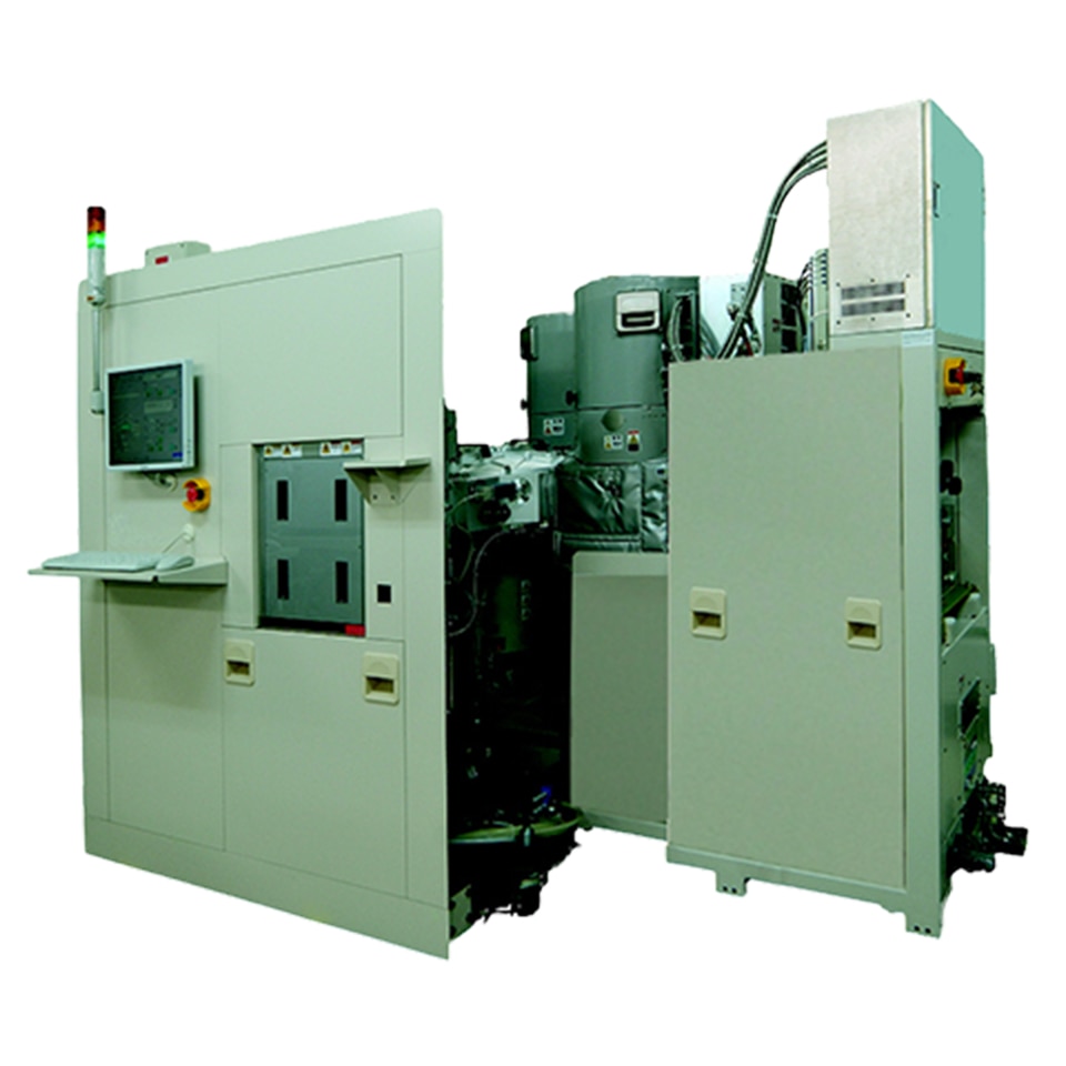
SPT’s Plasma Etching Technologies
SPT offers three types of plasma-based dry etching technologies, each optimized for different applications—from deep structures to delicate material release.
Deep Reactive Ion Etching (Si DRIE)
Si DRIE is a dry etching method used to create deep, narrow features in silicon with high aspect ratios and vertical sidewalls.
SPT’s Si DRIE systems are optimized for high-speed, high-precision silicon etching using the Bosch process.
They are ideal for MEMS and TSV fabrication, offering excellent uniformity, profile control, and depth accuracy.
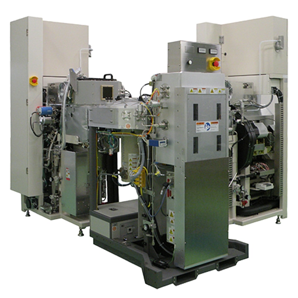
Reactive Ion Etching (RIE)
RIE is a plasma etching technique used to process hard-to-etch materials with directionality and fine control.
SPT’s RIE systems support precision etching of compound semiconductors, SiO₂, and other dielectrics, with excellent uniformity and low-damage processing.
Applications include power devices, photonic structures, and LED fabrication.
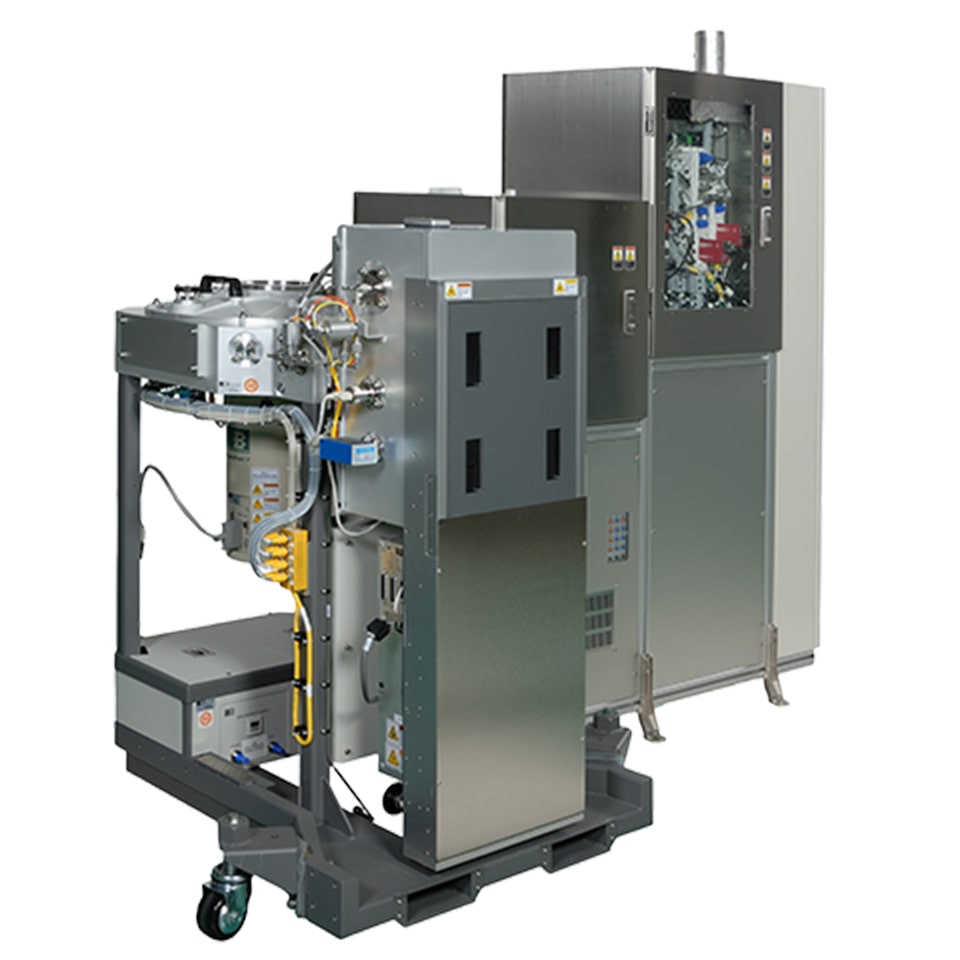
Sacrificial Layer Etching
Sacrificial layer etching removes buried silicon oxide layers to release MEMS structures without stiction.
SPT’s dry vapor-phase HF systems enable selective etching of sacrificial SiO₂ while preserving aluminum and other sensitive materials.
This approach ensures clean, damage-free release for critical MEMS components.
Why Choose SPT for Advanced Plasma Etching
SPT’s plasma etching systems are trusted by leading manufacturers for their precision, reliability, and proven performance across diverse semiconductor applications.
From deep silicon etching to delicate MEMS release, our technologies deliver uniform results, low process damage, and exceptional control.
Explore our lineup of Si DRIE, RIE, and sacrificial layer etching systems to find the solution that best fits your process needs.