PECVD
PECVD SPT’s PECVD systems deliver high-quality SiO₂ and SiN films with excellent step coverage, low stress, and fast deposition—ideal for MEMS, TSV, and power device applications.
Etching Overview
Plasma Enhanced Chemical Vapor Deposition (PECVD) is a widely used method for depositing thin dielectric films at low temperatures.
By introducing plasma energy into the reaction chamber, PECVD enables excellent film conformity, stress control, and high throughput.
SPT’s PECVD systems are optimized for advanced applications such as MEMS, TSV, and power semiconductors, where uniformity and reliability are critical.
What is PECVD in Semiconductor Manufacturing?
Plasma Enhanced Chemical Vapor Deposition (PECVD) is a process used to form thin films by introducing reactive gases into a vacuum chamber and energizing them with plasma.
The plasma breaks down gas molecules, allowing for film deposition on the wafer surface at relatively low temperatures—typically below 400°C.
PECVD is especially valuable in semiconductor manufacturing where temperature-sensitive structures, like MEMS and compound semiconductors, require conformal, high-quality films such as SiO₂ and SiN.
Types of CVD: PECVD, LPCVD, and APCVD
Chemical Vapor Deposition (CVD) methods vary in pressure, temperature, and energy source depending on how chemical reactions are initiated and films are formed.
The table below compares three commonly used CVD techniques—PECVD, LPCVD, and APCVD—each offering unique benefits for different semiconductor applications.
| Feature | PECVD | LPCVD | APCVD |
|---|---|---|---|
| Operating Temperature | Low (~150–400°C) | High (~500–800°C) | Medium–High (~400–500°C) |
| Deposition Rate | Medium–High | Medium | High |
| Conformality | Good (moderate aspect ratio coverage) | Excellent (high step coverage) | Fair (limited on complex structures) |
| Film Types | SiO₂, SiN, passivation, thick oxides | SiO₂, SiN, polysilicon | SiO₂, SiN, doped films |
| Process Control | Flexible, tunable via plasma parameters | Stable, thermally driven uniformity | Simple, less precise |
| Best Suited For | MEMS, TSV, power devices, compound semiconductors | Logic, MEMS, image sensors, advanced packaging | Fast oxide/nitride coatings on flat substrates |
Understanding the Strengths of PECVD, LPCVD, and APCVD
PECVD delivers low-temperature versatility, LPCVD offers excellent film conformity and uniformity, and APCVD provides speed and simplicity.
Each method supports different requirements in semiconductor manufacturing, from high-aspect MEMS to cost-efficient dielectric coatings.
PECVD uses plasma energy to enhance chemical reactions at low temperatures, enabling conformal deposition of SiO₂ and SiN films.
It is ideal for MEMS, TSV, and compound semiconductors where thermal budgets are limited.
SPT’s PECVD systems deliver excellent film quality, step coverage, and stress control across various substrate types.
LPCVD deposits thin films using thermal reactions at low pressure, resulting in highly conformal and uniform layers across complex wafer topographies.
It is ideal for SiO₂, SiN, and polysilicon deposition in MEMS, image sensors, and logic devices requiring consistent step coverage and film quality.
Though slower than APCVD, LPCVD balances performance and throughput for advanced applications.
APCVD forms films through thermal decomposition of precursor gases at atmospheric pressure.
It offers high throughput and simple system design, making it suitable for large-area coatings and cost-sensitive applications.
SPT supports Watkins-Johnson (WJ) legacy APCVD systems, offering continued performance with factory-certified upgrades and spare parts.
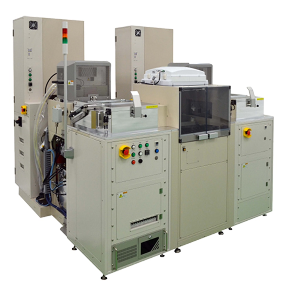
SPT’s PECVD Technologies
SPT provides plasma-enhanced and thermal CVD systems tailored for high-quality dielectric film deposition across MEMS, TSV, and power semiconductor applications.
Plasma Enhanced CVD (PECVD)
SPT’s PECVD systems enable low-temperature deposition of high-quality SiO₂ and SiN films with excellent conformality and low residual stress.
Our tools are optimized for demanding processes in MEMS, TSV, and compound semiconductor devices, where thermal budgets and film performance are critical.
With flexible handling options from R&D to high-volume manufacturing, SPT PECVD ensures consistency, productivity, and ease of integration.
Why Choose SPT for PECVD
SPT’s PECVD systems are trusted for their reliability, low-temperature performance, and precision across a wide range of semiconductor applications.
From MEMS and TSV to power devices, our deposition technologies deliver uniform films, low particle levels, and stable operation for both R&D and production environments.