Advanced Packaging
Advanced Si DRIE and PECVD Solutions for Through-Silicon Via (TSV) Integration
TSV-Based Advanced Packaging: Enabling High-Density, High-Speed Device Performance
Three-dimensional (3D) packaging technologies—particularly through-silicon vias (TSVs)—are essential for achieving higher performance in advanced semiconductor devices. From high-performance computing (HPC) and mobile applications to emerging AI and edge devices, TSVs support faster interconnects, smaller footprints, and improved energy efficiency.
As the semiconductor industry continues to scale vertically, the need for precise, high-speed, and low-damage processing of TSV structures becomes increasingly critical.
Key Challenges in TSV Fabrication for Advanced Packaging
TSV structures introduce unique demands on equipment performance and process control. Key challenges include:
-
- Etch speed and uniformity:
- TSVs often require deep, high-aspect-ratio vias that must be etched through silicon with both speed and consistency. Throughput is essential, especially for volume manufacturing.
-
- Process choice:
- Bosch vs. non-Bosch Process: While both techniques are used, the Bosch process offers superior sidewall protection and etch control for deep structures—making it a preferred option for TSV fabrication in many applications.
-
- Thermal budget limitations:
- Subsequent bonding or metallization steps often require low thermal budgets. This necessitates dielectric deposition processes that maintain film quality at lower temperatures.
-
- Profile control and residue minimization:
- Minimizing scalloping, bowing, and polymer buildup is critical to maintain electrical and structural integrity.
SPT’s Etching and Deposition Solutions for TSV Applications
SPT provides specialized Si DRIE and PECVD systems engineered to meet the precision, throughput, and reliability requirements of advanced Advanced packaging.
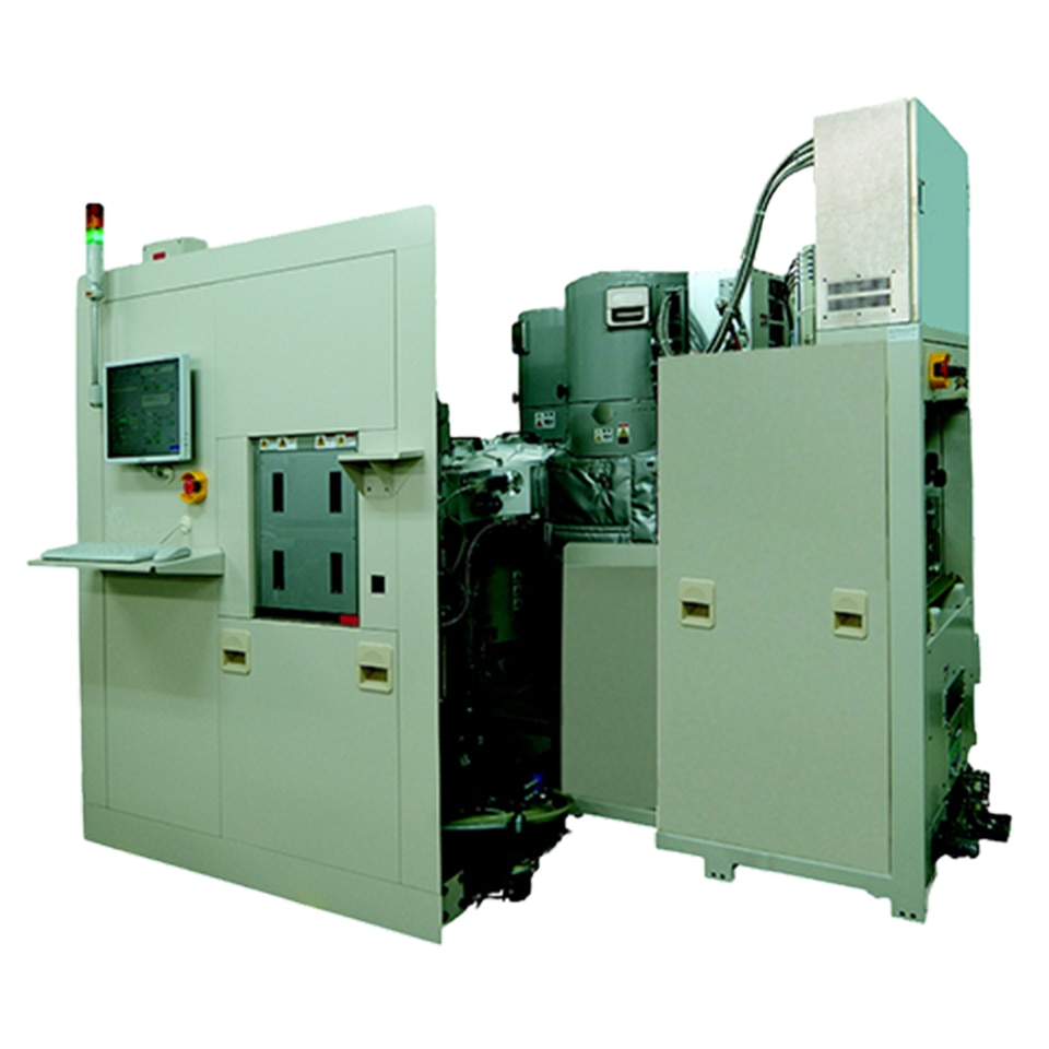
1. Silicon Deep Reactive Ion Etching (Si DRIE)
- High-speed silicon etching using the Bosch process
- Excellent sidewall protection with minimal scalloping
- Stable performance over deep vias and thick substrates
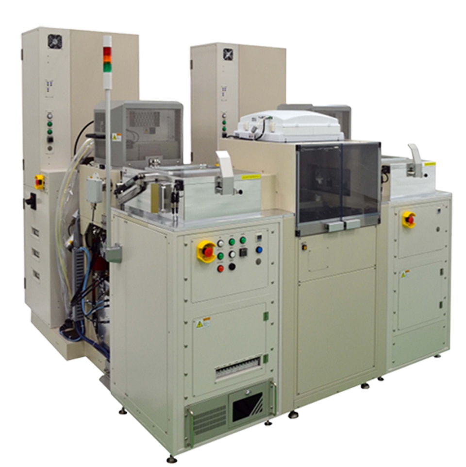
2. Low-Temperature PECVD
SPT’s plasma etchers deliver:
- High-quality SiO₂ and SiNₓ films at reduced thermal budgets
- Precise thickness and stress control for interlayer dielectrics
- Ideal for TSV insulation and passivation steps
Explore TSV Process Steps with SPT
See how SPT supports each critical stage in TSV-based Advanced packaging.
Each card below links to a matching tool or capability.