RF Devices
Low-Damage Etching and Deposition for High-Frequency GaN Semiconductor Applications
GaN-HEMT: Powering High-Frequency Performance in a Compact Form Factor
GaN-based high electron mobility transistors (GaN-HEMTs) are essential for next-generation RF applications, including 5G communication, satellite systems, radar, and high-efficiency power amplifiers. These devices deliver high-frequency performance, power density, and thermal reliability far beyond what conventional silicon technologies can achieve.
As demand accelerates across Asia and global growth markets, device manufacturers must address new process challenges to ensure yield, consistency, and device reliability—especially in mass production environments.
Key Challenges in GaN-HEMT Device Fabrication
Manufacturing GaN-HEMT devices requires careful process control across multiple layers and interfaces. Critical challenges include:
-
- Etching control of GaN and AlGaN layers:
- High selectivity and damage minimization are essential to avoid impacting active layers, especially when dealing with compound structures and thin films.
-
- Preserving the 2DEG channel:
- Plasma-induced damage or stress can degrade the two-dimensional electron gas (2DEG) that enables GaN-HEMT performance. Low-damage processing is key to maintaining high carrier mobility.
-
- Surface passivation and insulation:
- Deposited films must be uniform, low-stress, and thermally stable to isolate RF structures and enhance breakdown voltage.
-
- High-speed backside via etching:
- For devices requiring back-side metallization or thermal management vias, fast and uniform etching through GaN or other materials is required.
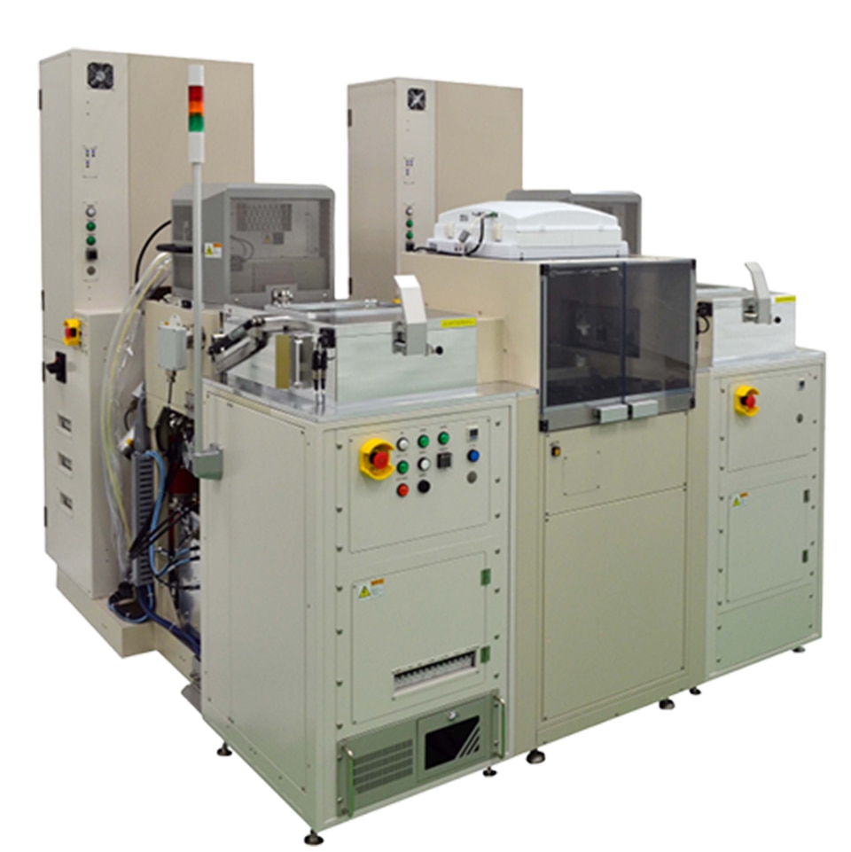
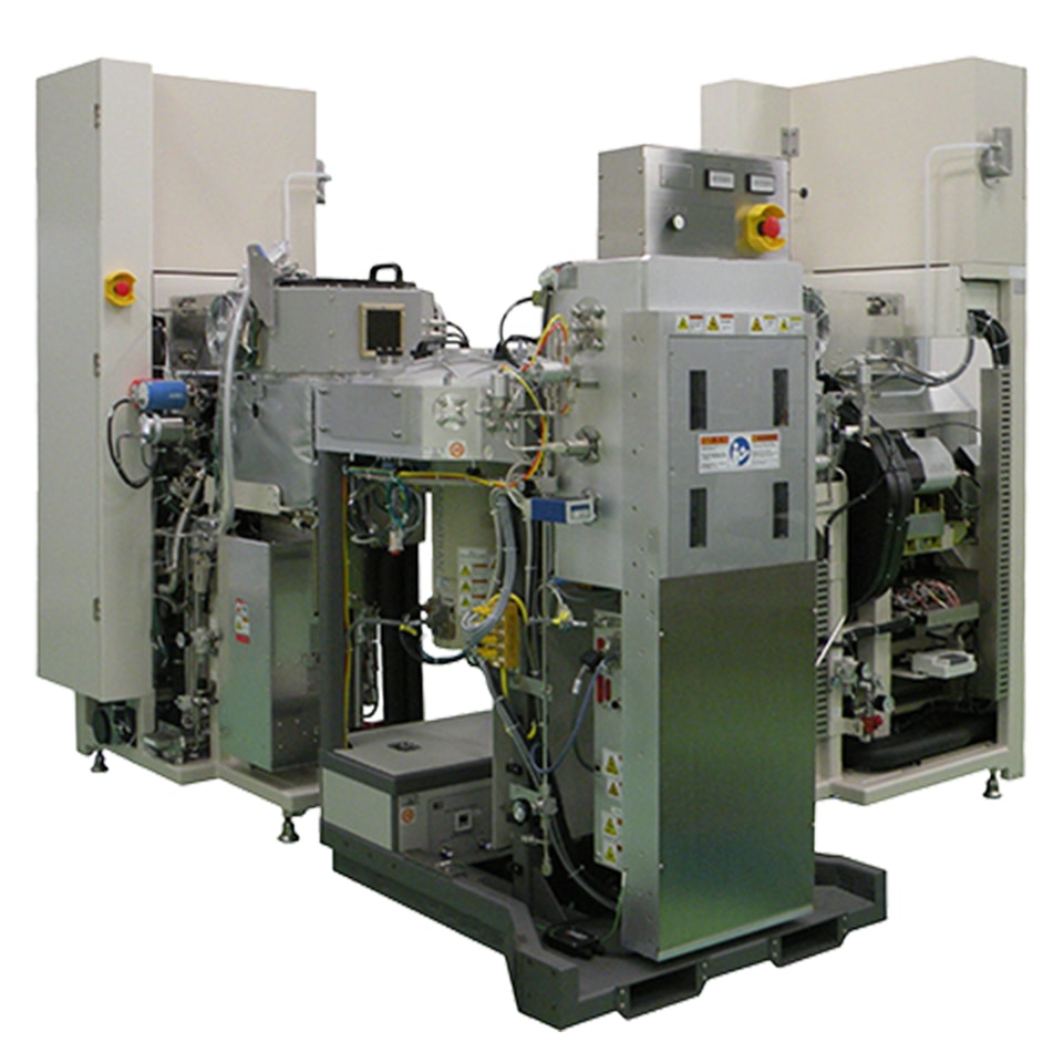
SPT’s Low-Damage Solutions for GaN-HEMT Processing
SPT provides plasma etching and PECVD systems engineered to meet the unique demands of GaN-based HEMT devices with an emphasis on precision, repeatability, and damage mitigation.
1. Low-Damage Etching for GaN/AlGaN
- High-selectivity etching of GaN/AlGaN without damaging underlying 2DEG
- Smooth sidewalls with minimal surface roughness
- Excellent control over mesa, gate, and via structures
2. Low-Temperature, High-Quality PECVD
- Formation of passivation and insulation films (e.g., SiNₓ) with low ion damage
- Optimized for high breakdown voltage and thermal stability
- Tunable stress control for high-frequency substrates
3. High-Speed Backside Via Etching
- Etching of through-substrate vias for heat dissipation or interconnects
- Consistent etch rate across large wafers with minimal taper
Explore GaN-HEMT Device Processing with SPT
See how SPT supports each critical step in GaN-HEMT fabrication — from passivation to precision etching.
Browse the process flow below to explore solutions optimized for high-frequency device integration.