LED Devices
Precision Etching and PECVD Solutions for MicroLED and Laser Applications
MicroLED and Laser Devices: Driving the Next Generation of Display and Optical Technology
MicroLEDs and GaN-based laser devices are at the forefront of high-performance display and optical systems. Offering exceptional brightness, power efficiency, and form factor flexibility, these devices are rapidly advancing in sectors ranging from AR/VR and smartphones to automotive and biomedical technologies.
As device miniaturization accelerates and integration density increases, manufacturers face new challenges in achieving high yield, precision, and surface integrity across complex materials like GaN and sapphire.
Key Challenges in MicroLED and Laser Device Fabrication
Producing high-quality microLED and GaN laser devices requires overcoming several critical process challenges:
-
- GaN layer etching:
- GaN is chemically stable and difficult to etch with precision. Controlling sidewall angle, selectivity, and surface damage is essential for electrical performance and yield.
-
- Sapphire substrate processing:
- Sapphire wafers used for epitaxial growth are mechanically hard and must be processed without inducing cracks or delamination. Smooth surface finishing and low-defect rates are key.
-
- Thin film uniformity:
- Dielectric and passivation films must be deposited with consistent thickness across small and densely patterned areas, requiring advanced PECVD process control.
-
- Damage-sensitive structures:
- As device sizes shrink, any process-induced roughness or plasma damage can lead to significant performance degradation or early failure.
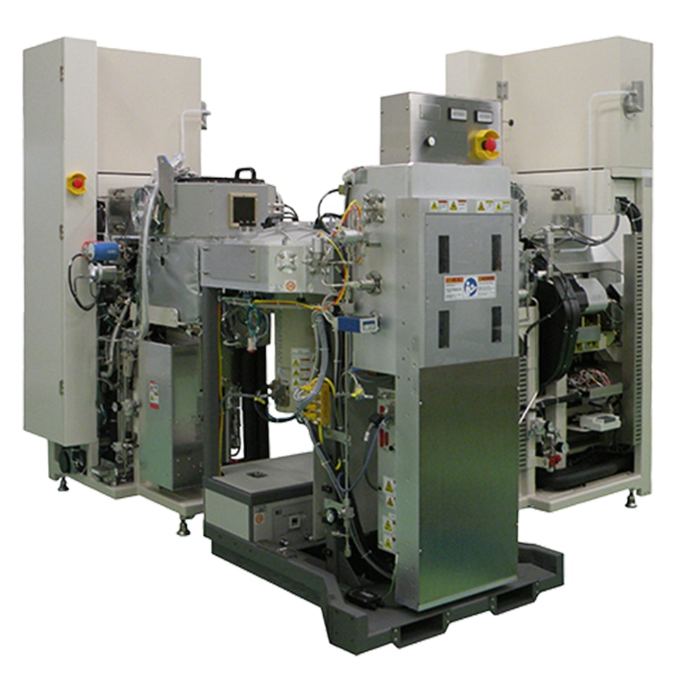
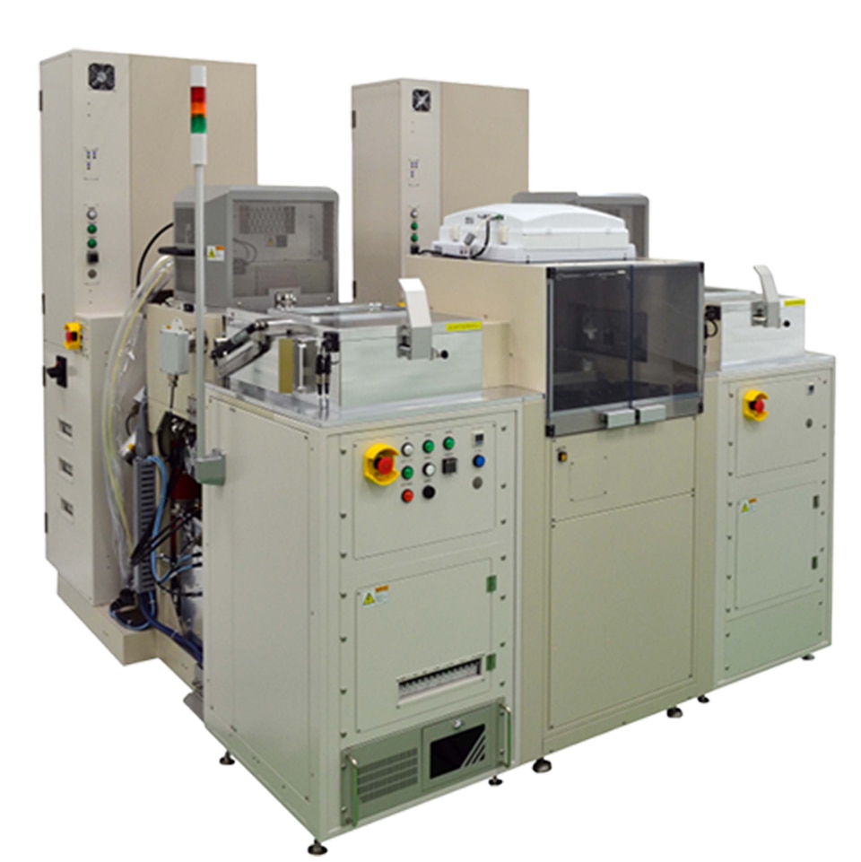
SPT’s Etching and Deposition Solutions for LED Manufacturing
SPT offers specialized dry etching and low-temperature PECVD technologies designed to meet the demands of high-precision LED device fabrication.
1. Etching Solutions
- High-selectivity etching for GaN and AlGaN layers
- Precise anisotropic control for deep trenches and mesa structures
- Surface damage minimization for higher yield and reliability
- Sapphire substrate processing with excellent uniformity
2. PECVD Solutions
- Uniform deposition of high-quality SiO₂ and SiNₓ on GaN and sapphire
- Excellent step coverage across micro-structures
- Low-temperature processing ideal for thermally sensitive LED substrates
Explore LED Process Steps with SPT
Discover how SPT supports each critical stage in LED device manufacturing.
Each card below links to our relevant tools and technologies.