MEMS Devices
High-Precision Etching and Deposition for Advanced MEMS Structures
MEMS Applications and Industry Trends
Micro Electro Mechanical Systems (MEMS) are essential components in today’s smart technologies—ranging from smartphones and automotive sensors to medical diagnostics, industrial automation, and RF systems.
As MEMS devices become smaller, more complex, and more functionally integrated, manufacturers face growing demands for high-precision processes and ultra-clean surfaces across various layers and materials.
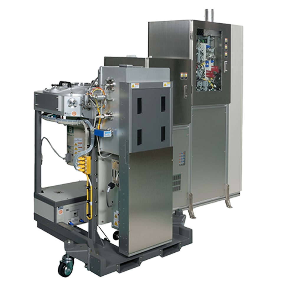
SPT supports MEMS innovation with advanced etching, deposition, and thermal processing systems tailored for fine-featured structures and mass production requirements.
Key Challenges in MEMS Fabrication
MEMS manufacturing involves complex multi-layer structures, often with deep cavities, thin films, and sacrificial layers. Major technical challenges include:
-
- Deep silicon etching with high aspect ratios:
- MEMS structures often require etching depths over 100 μm while maintaining vertical sidewalls and precise profiles.
-
- Thin film stress control:
- Films deposited by PECVD or LPCVD must offer low residual stress, excellent step coverage, and uniformity to ensure device reliability.
-
- Multi-layer alignment and integration:
- As MEMS designs become more functional, precise control over deposition and etch-back of structural and sacrificial layers is essential.
-
- Surface quality and consistency:
- Smooth etched surfaces, minimized tilting or notching, and reproducible results across wafer lots are critical for yield.
Etching & Deposition Solutions for MEMS Processing
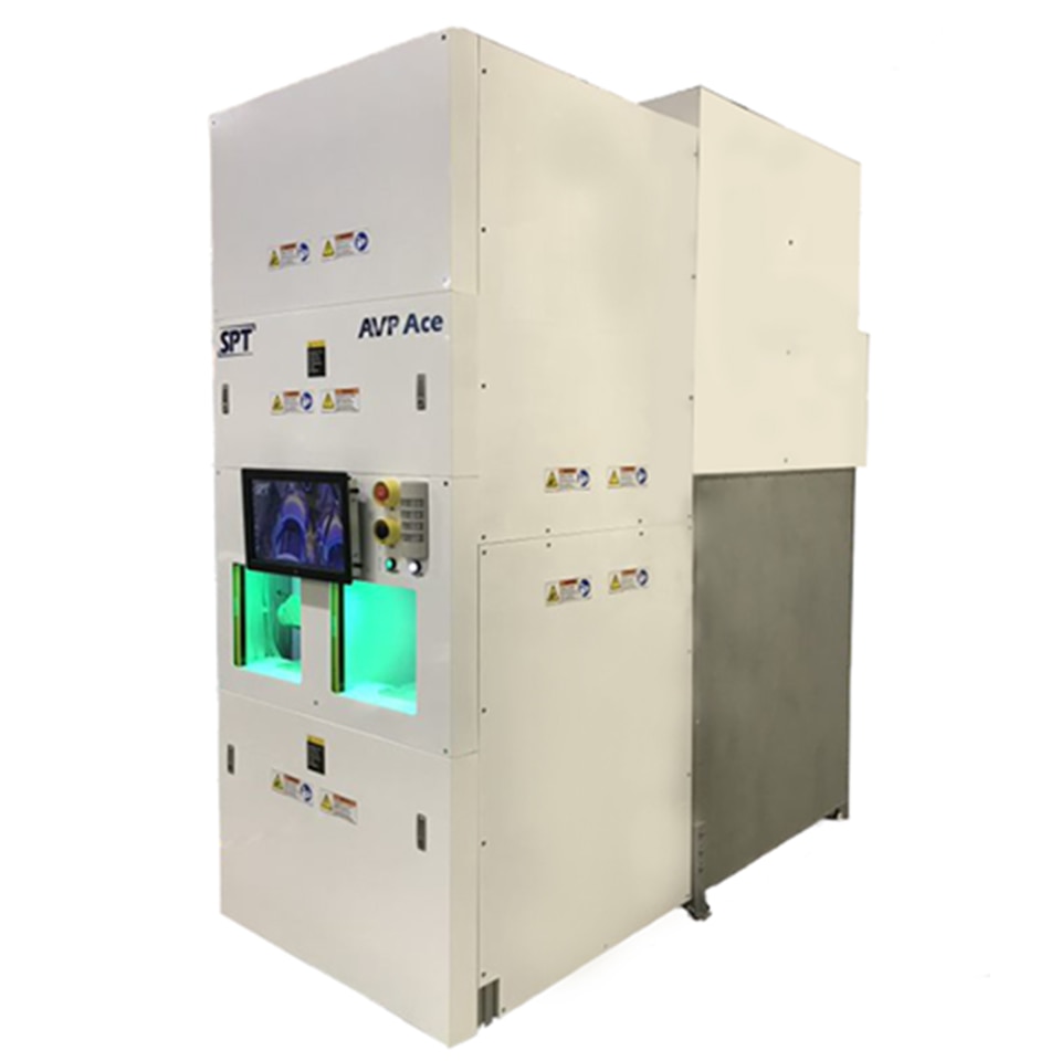
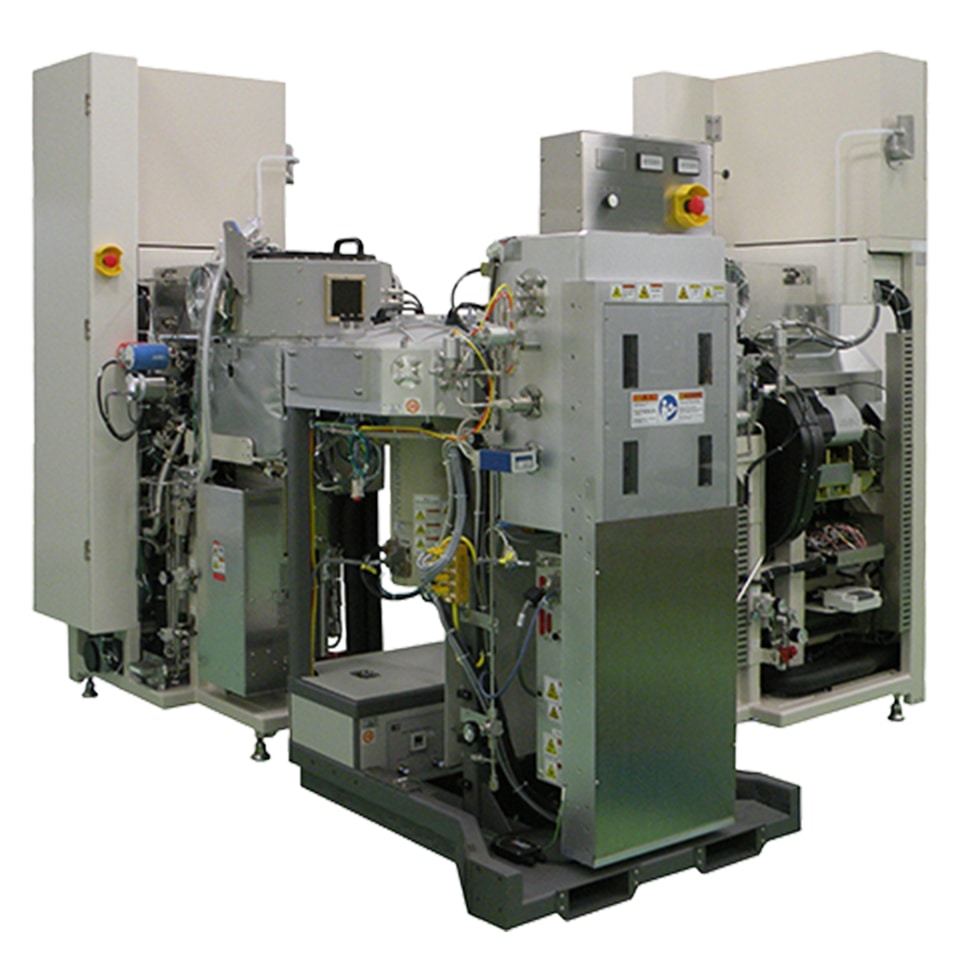
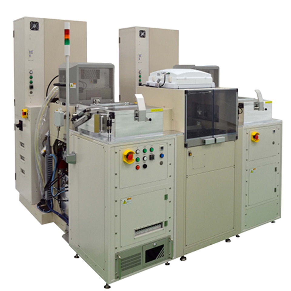
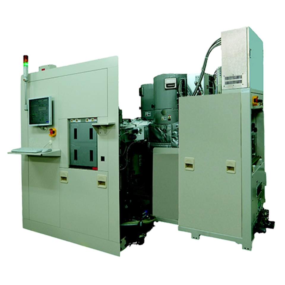
SPT offers a broad portfolio of systems optimized for MEMS manufacturing, enabling stable, scalable, and high-precision processing across etch and deposition steps.
1. Deep Silicon Etching (Si DRIE)
- High-aspect ratio etching with minimal profile distortion
- Excellent sidewall control and low undercut for cavity structures
- Ideal for microphones, pressure sensors, and inertial MEMS
2. PECVD for Stress-Sensitive Thin Films
- Precise stress tuning across SiO₂ and SiNₓ films
- Low-temperature deposition with high step coverage
- Optimized for structural and passivation layers in MEMS stacks
Explore MEMS Process Steps with SPT
SPT supports every step of the MEMS process flow, from etching deep structures to forming high-quality dielectric films.