SiC Power Devices
Advanced Etching and PECVD Solutions for Next-Generation Power Semiconductor Devices
SiC Power Devices: Applications and Industry Trends
Power devices, especially wide-bandgap semiconductors like SiC (Silicon Carbide), are revolutionizing the way we manage power in electric vehicles (EVs), renewable energy systems, industrial equipment, and data centers. These components enable faster switching speeds, higher voltage endurance, and greater energy efficiency than traditional silicon-based devices. As demand for power-efficient systems continues to surge, the need for reliable, scalable, and precise semiconductor fabrication solutions grows accordingly.
Key Challenges in SiC Power Semiconductor Manufacturing
SiC-based power devices offer high performance, but their manufacturing presents unique technical difficulties. Some of the key challenges include:
-
- Hard material processing:
- SiC’s extreme hardness and chemical resistance make it difficult to etch using standard plasma techniques. Specialized dry etching methods are essential to achieve precise patterning without substrate damage.
-
- Thick film deposition:
- Power devices often require thick dielectric layers (e.g., SiO₂, SiN) for isolation and protection. These layers must exhibit excellent uniformity, step coverage, and low defectivity.
-
- Thermal sensitivity:
- Excess heat during processing can degrade wafer integrity and impact device reliability. Controlled low-temperature processes are vital for maintaining uniformity and reducing thermal stress.
-
- High aspect ratio structures:
- Deep trenches and isolation features require highly anisotropic etching with excellent sidewall control and minimal roughness.
-
- Yield and reliability:
- To meet volume demands, processes must be repeatable, scalable, and resistant to defect generation or contamination.
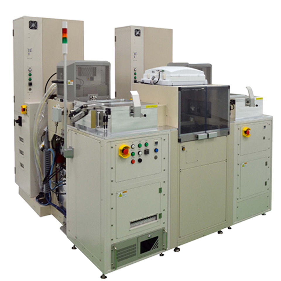
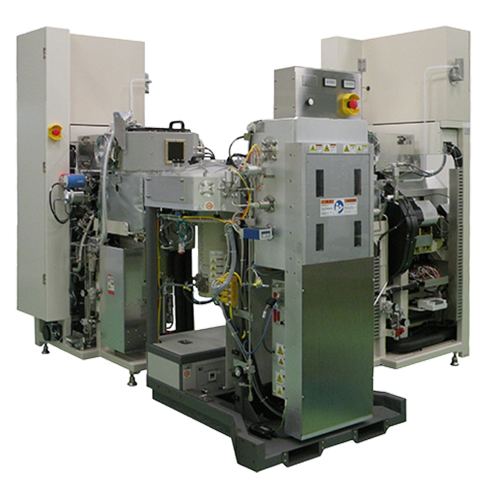
Etching & PECVD Solutions for SiC Power Device Processing
SPT provides specialized equipment and process know-how to overcome the toughest challenges in SiC power device manufacturing.
1. PECVD Solutions
Our PECVD systems are optimized for:
- Low-temperature deposition of high-quality SiO₂ and SiNₓ films
- Excellent conformality on thick and uneven topographies
- Tight film thickness control across large-diameter wafers
These capabilities are crucial for passivation layers, interlayer dielectrics, and surface protection in high-voltage power ICs.
2. Etching Solutions
SPT’s plasma etchers deliver:
- Highly selective dry etching of SiC and other wide-bandgap materials
- Smooth, vertical sidewalls with minimal substrate damage
- Robust process control for consistent, high-yield results across wafer batches
Our systems support both research and high-volume production, with scalable configurations tailored to your specific needs.
Explore SiC Power Device Processing with SPT
See how SPT supports each key step in SiC power device fabrication.
Browse the process flow below and discover matching etching and deposition solutions.