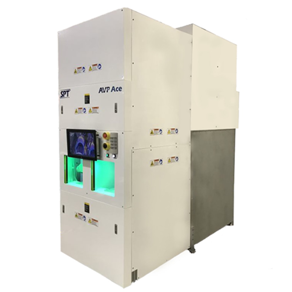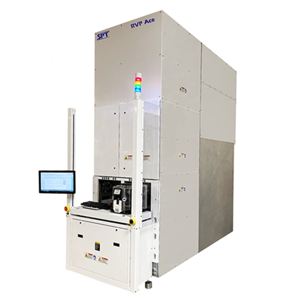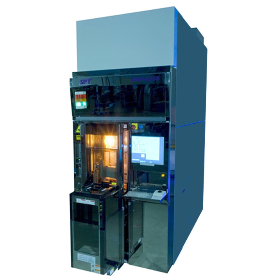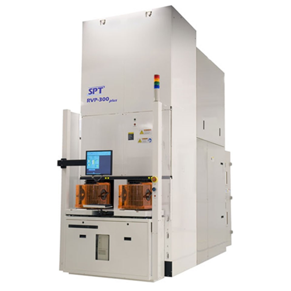
Vertical Batch Furnace
Thermal Processing Overview
Vertical batch furnaces are essential thermal processing systems in semiconductor manufacturing, enabling key processes such as diffusion, oxidation, annealing, and chemical vapor deposition (LPCVD, APCVD).
By utilizing precise temperature control and batch wafer handling, these furnaces deliver exceptional uniformity, high throughput, and stable process conditions.
SPT’s vertical batch systems are designed for advanced device fabrication, including MEMS, power semiconductors, and other high-performance applications that require reliable, scalable thermal processing—complementing our plasma-based etching and deposition solutions.
What is Thermal Processing in Semiconductor Manufacturing?
Thermal processing refers to the use of controlled heating techniques to modify material properties during semiconductor fabrication.
This includes key processes such as diffusion, oxidation, annealing, and chemical vapor deposition, where temperature, ambient gases, and time are precisely managed.
In semiconductor manufacturing, thermal processing enables critical functions like dopant activation, film growth, and defect repair—making it essential for producing high-performance, reliable devices.
Types of Thermal Processing: Anneal, Diffusion, Oxidation, LPCVD, and APCVD
Thermal processing methods vary in temperature, ambient conditions, and process objectives—ranging from dopant activation to thin film deposition.
The table below compares five widely used techniques in semiconductor manufacturing, each essential for achieving high-performance device structures.
| Feature | Anneal | Diffusion | Oxidation | LPCVD | APCVD |
|---|---|---|---|---|---|
| Purpose | Activate dopants, relieve stress, repair defects | Introduce dopants into silicon | Grow SiO₂ on silicon surface | Deposit thin films at low pressure | Deposit films at atmospheric pressure |
| Typical Temperature | 400–1100°C | 800–1100°C | 800–1100°C | 500–800°C | 400–500°C |
| Process Gases | Inert gas (e.g. N₂, Ar) | Oxygen or dopant gas (e.g. POCl₃, BBr₃) | O₂ or H₂O vapor (dry/wet oxidation) | Silane, dichlorosilane, NH₃, etc. | Silane, ozone, TEOS, etc. |
| Key Applications | Logic devices, power semiconductors | CMOS, image sensors, discrete devices | Isolation layers, gate oxides | SiN, SiO₂, poly-Si for MEMS, ICs | Passivation, dielectric layers |
Process Highlights: Key Thermal Techniques Explained
Thermal processing covers a wide range of techniques, each serving a specific role in semiconductor fabrication.
The tabs below provide an overview of five essential processes—annealing, diffusion, oxidation, LPCVD, and APCVD—highlighting how they work and where they are commonly used.
Annealing is a thermal process used to activate dopants, relieve stress, and repair crystal defects in semiconductor wafers.
It involves heating wafers in an inert atmosphere, typically between 400°C and 1100°C.
Annealing is commonly used after ion implantation and etching in logic devices, power semiconductors, and MEMS..
Diffusion forms films through thermal decomposition of precursor gases at atmospheric pressure.
It offers high throughput and simple system design, making it suitable for large-area coatings and cost-sensitive applications.
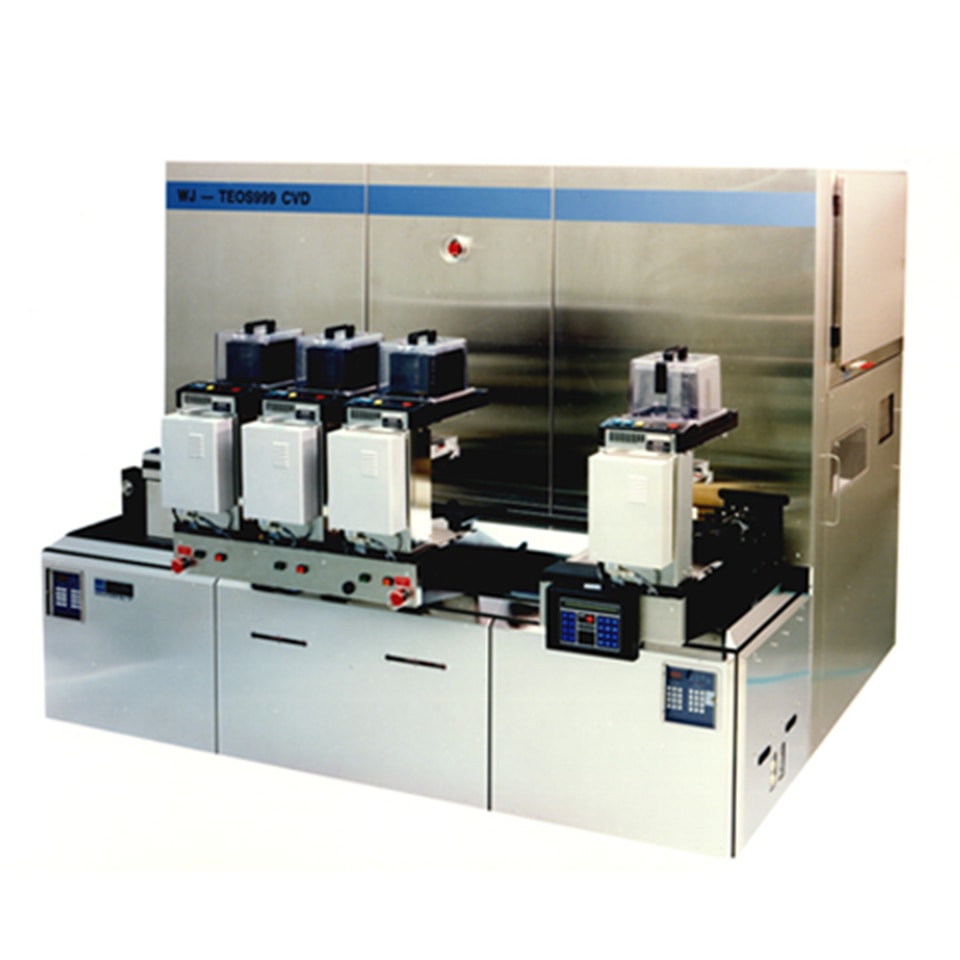
SPT supports Watkins-Johnson (WJ) legacy APCVD systems, offering continued performance with factory-certified upgrades and spare parts.
Oxidation forms a silicon dioxide (SiO₂) layer by exposing wafers to oxygen or steam at elevated temperatures.
This can be done as dry or wet oxidation depending on the ambient.
SiO₂ is essential for gate insulation, surface passivation, and isolation structures.
Low Pressure Chemical Vapor Deposition (LPCVD) deposits thin films at reduced pressure and moderate temperatures (500–800°C).
It enables excellent uniformity and step coverage for SiN, SiO₂, and polysilicon layers.
LPCVD is key for MEMS, logic, and advanced packaging.
Atmospheric Pressure CVD (APCVD) deposits films at ambient pressure using reactive gases like silane and ozone.
It is a fast, high-throughput method used for passivation and dielectric layers.
APCVD suits applications with relaxed step coverage requirements.
Why Choose SPT for Vertical Batch Furnaces
SPT’s vertical batch furnaces are trusted for their uniformity, process stability, and scalability across a wide range of thermal applications.
From MEMS and image sensors to power devices, our systems deliver consistent results for diffusion, oxidation, annealing, and CVD—supporting both R&D and high-volume production with reliable batch performance.